Mastering ESD protection techniques to improve the reliability of electronic products
In ESD damage, static electricity can cause catastrophic damage to I/O ports, potentially leading to data bit ghosting, product damage, and even causing electronic device "hard faults" or component damage. So engineers need to consider ESD issues in the design and master the solutions.
Currently, more and more portable products are using low-power logic chips, which are highly sensitive to ESD due to the limitations of metal oxide semiconductor (MOS) dielectric breakdown and bipolar reverse junction current. IC chips that control I/O ports (USB ports, Ethernet ports, etc.) are no exception, as most of them are designed and manufactured based on CMOS technology, which makes IC chips very sensitive to damage caused by ESD. In addition, most I/O ports (especially USB ports) are hot swappable systems, which are highly susceptible to ESD effects caused by user or air discharge. It can be seen that ESD protection is essential in today's portable and USB applications.
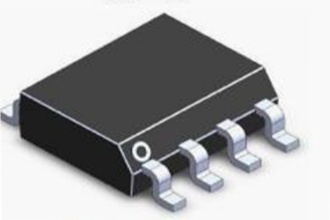
Some engineers have raised questions about the protective effect of adding TVS devices in the T1/E1 interface design. They believe that adding TVS devices on the power line can help solve ESD problems from the power port, and emphasize that TVS should be connected to the power supply's VCC and ground to prevent ESD interference from the power supply.
When answering engineers' questions about considering ESD protection comprehensively, three aspects should be taken into account: 1. The ESD capacity of the chip; 2. PCB layout design; 3. Mechanical design. He stated that a good PCB layout design should strive to increase the grounding area and shorten the PCB routing. He particularly emphasized that TVS arrays can effectively solve ESD problems.
In response to common mode interference caused by ESD, common mode chokes or TVS arrays can usually be used to solve ESD problems and complete EMI filtering. The common mode chokes are connected in series in the circuit, and the TVS is connected in parallel in the circuit. In addition to considering using devices to solve ESD problems, we can also follow some basic rules to solve PCB ESD problems:
1. Try to use multi-layer PCBs as much as possible. Compared to double-sided PCBs, the ground plane, power plane, and closely arranged signal ground spacing can reduce common impedance and inductive coupling, achieving 1/10 to 1/100 of that of double-sided PCBs.
2. Try to place each signal layer as close as possible to a power or ground layer. For high-density PCBs with components on both the top and bottom surfaces, short connection lines, and many filling grounds, inner layer lines can be considered. Most signal lines, as well as power and ground planes, are located on the inner layer, resembling Faraday boxes with shielding capabilities.
3. For double-sided PCBs, tightly interwoven power and ground grids should be used. The usual solution principle is to go through a cycle of testing, problem-solving, and retesting, where each cycle may affect the design of at least one PCB. In the PCB design process, most design modifications can be limited to adding or removing components through prediction.
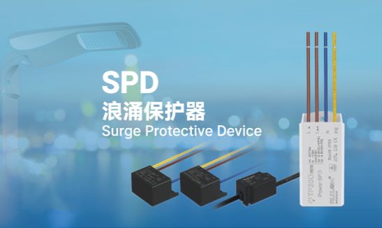
, Thermistor, Transient Suppressor Diode (TVS), Ceramic Gas Discharge Tube (GDT), Surge Protective Device (SPD), Composite Protective Unit (KOV), Electrostatic Discharge Array (ESD), Self healing Fuse (PTC), etc&desc=Dongguan Rongchang Technology Co., Ltd. )